
Samsung and Cadence Partnership Redefines Semiconductors for AI Robots and Cars Through Co-Design

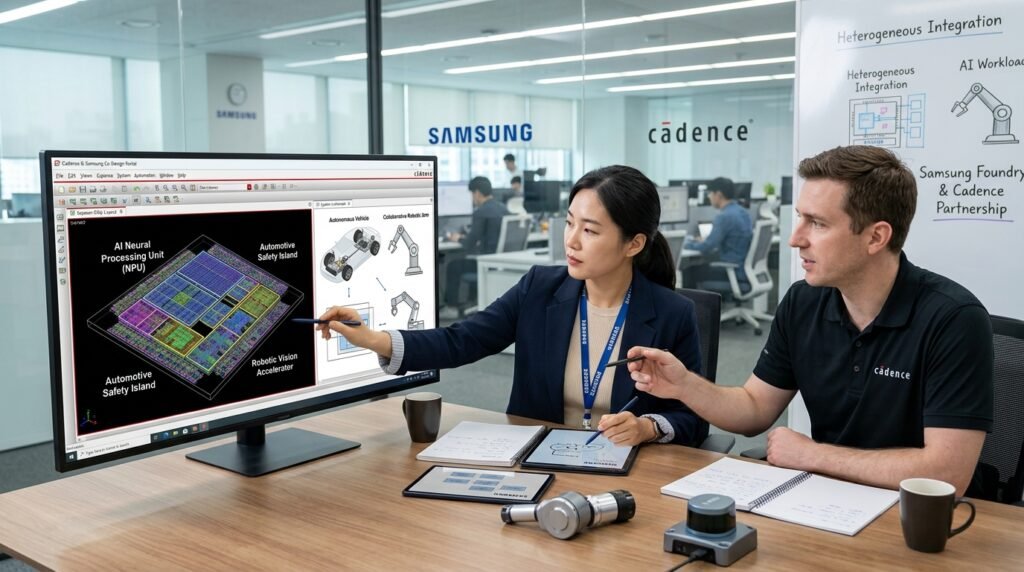
Samsung and Cadence Partnership Redefines Semiconductors for AI Robots and Cars is a strategic shift in chip design and manufacturing: Samsung contributes advanced semiconductor process and foundry capabilities, while Cadence provides electronic design automation (EDA), IP, and system-level verification tools that help engineers build faster, safer, and more efficient chips for physical AI workloads. In technical terms, this is not a marketing alliance; it is a co-optimization effort across design, packaging, verification, and manufacturing.
That matters now because robots and AI-defined vehicles do not behave like conventional consumer devices. They process sensor streams, run inference locally, react to latency-sensitive events, and operate under tighter thermal and power limits. In practice, the chip stack has to handle camera data, radar, lidar, and control loops without wasting energy or introducing delays. The Samsung and Cadence Partnership Redefines Semiconductors for AI Robots and Cars because it targets the exact bottlenecks that usually slow deployment: design complexity, memory bandwidth, packaging constraints, and validation time.
There is also a commercial reality behind the technical one. Automotive OEMs, robotics companies, and hyperscale AI teams increasingly want domain-specific silicon instead of generic compute. A collaboration between a leading foundry and a leading EDA vendor can shorten the path from architecture concept to qualified product. That does not guarantee success in every use case, and some workloads still fit off-the-shelf silicon better, but the direction is clear: physical AI is pushing semiconductors toward tighter integration and more aggressive co-design.
Key Takeaways
- The Samsung-Cadence collaboration links design software and manufacturing capability, which is where most advanced chip programs now win or fail.
- Robots and AI cars need low-latency, power-efficient, and safety-aware silicon, not just raw compute throughput.
- Chiplets, advanced packaging, and system-level verification are becoming central to next-generation automotive and robotics platforms.
- Physical AI raises the bar for thermal control, memory bandwidth, and deterministic performance under real-world conditions.
- The partnership is strategically important because it compresses development cycles and reduces risk before tape-out and qualification.
Samsung and Cadence Partnership Redefines Semiconductors for AI Robots and Cars Through Co-Design
What the Partnership Actually Is
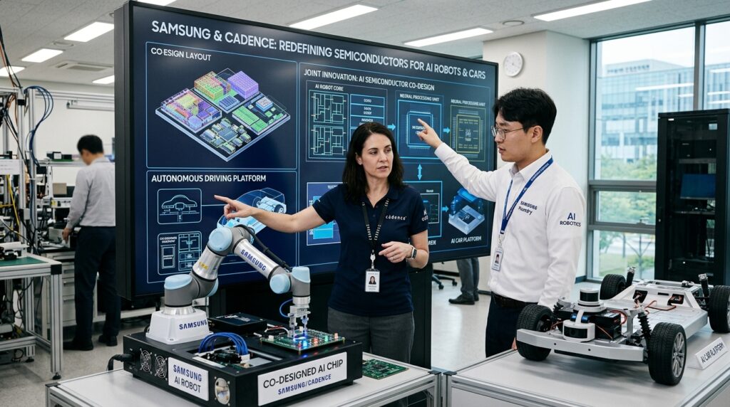
Formally, this kind of alliance combines semiconductor foundry expertise with EDA and IP tooling to optimize a chip from architecture to manufacturing. Samsung supplies process technologies, advanced nodes, and packaging capabilities; Cadence supplies the software environment used to model, verify, and sign off the design. The result is a co-design workflow, where engineers tune silicon, interconnect, memory hierarchy, and package characteristics together instead of treating each layer separately.
That distinction matters. Traditional chip development often breaks down when teams optimize only one layer, such as compute density, while ignoring heat, signal integrity, or board-level constraints. The partnership aims to reduce those blind spots. In physical AI, that is not optional. A robot controller or autonomous-driving domain compute unit must survive vibration, temperature swings, strict latency budgets, and long qualification cycles.
Why Robotics and Automotive Are Driving This Change
Robots and smart vehicles share a common requirement: they must perceive, decide, and act in near real time. A factory robot, for example, may fuse multiple cameras and motion sensors while controlling motors with microsecond-level timing. An AI vehicle may run perception, localization, sensor fusion, path planning, and safety monitoring in parallel. Generic chips can do part of the job, but they rarely do all of it with the efficiency these systems need.
Who works in this field knows the pain points. A design that looks strong in a benchmark can fail in the lab because memory traffic spikes, thermal limits kick in, or timing closure slips late in the flow. That is why co-optimization between foundry and EDA matters: it aligns what is possible in silicon with what the system actually needs on the road or on the factory floor.
The Role of Cadence in the Modern Design Flow
Cadence’s value sits in the middle of the pipeline. Its tools are used for RTL design, simulation, formal verification, physical implementation, and package-aware analysis. In advanced programs, that means engineers can evaluate a design long before it becomes an expensive wafer run. For AI accelerators and automotive SoCs, this shortens iteration loops and reduces the chance of discovering a fatal flaw after manufacturing begins.
One practical benefit is improved signoff confidence. When a team can model timing, power, and thermal behavior early, it can make smarter tradeoffs between clock speed, memory placement, and interconnect topology. That is why the collaboration is more than an announcement about two companies working together; it is a mechanism for lowering engineering risk in some of the hardest semiconductor categories.
Why Physical AI Needs a Different Semiconductor Strategy
Physical AI is Harder Than Cloud AI
Physical AI refers to AI systems that interact directly with the physical world through sensors and actuators. Unlike a data-center model that can tolerate high latency or cloud dependence, a robot or car must respond immediately and predictably. That means the chip must deliver not only throughput, but determinism. A delayed decision in a warehouse robot can cause downtime; in an autonomous vehicle, it can create a safety issue.
This is why edge inference, sensor fusion, and control logic are becoming tightly integrated inside the same silicon ecosystem. The challenge is not just computing the model. It is moving data quickly enough, keeping power under control, and ensuring the output arrives when the system expects it. In that environment, every nanosecond and every milliwatt matter.
Why Chiplets and Advanced Packaging Matter Here
Chiplets allow designers to split a large system into smaller functional blocks connected through high-bandwidth links. That approach can improve yield, flexibility, and product scaling. Advanced packaging takes this further by enabling dense interconnects between compute, memory, and I/O dies. For AI robots and cars, the packaging layer is no longer a back-end detail; it is part of the architecture.
Samsung’s foundry and packaging capabilities make this especially relevant. When paired with Cadence’s multi-die design and analysis tools, teams can evaluate signal integrity, thermal hotspots, and power delivery across a full package rather than a single die. The payoff is architectural freedom. Engineers can mix and match compute blocks instead of forcing every function onto one monolithic chip.
Design Challenge Why It Matters in AI Robots and Cars What the Samsung-Cadence Stack Addresses Latency Control loops and perception pipelines must react immediately Early timing analysis and system-level co-design Power Edge platforms run under strict thermal and battery limits Power-aware implementation and process optimization Memory bandwidth Sensor fusion and AI inference move large data volumes Multi-die planning and package-aware validation Safety Failures in automotive and robotics systems can be costly or dangerous Verification, signoff, and reliability-focused design flows
The Real Bottleneck is Not Just Compute
A common mistake is to assume AI hardware problems are solved by adding more TOPS. They are not. The bottleneck often shifts to memory access, interconnect efficiency, software toolchains, and validation time. A robot may need modest model size but extremely fast and consistent response. A vehicle may need multiple inference engines plus safety logic, yet still remain thermally stable in a summer parking lot.
That is why the industry is moving away from simple “bigger chip, faster chip” thinking. The winning approach is system balance. Samsung and Cadence are positioned around that reality: one side links the design intent to manufacturing capability, the other side makes the design usable before it reaches silicon.
What Samsung Brings: Foundry Scale, Packaging, and Manufacturing Discipline
Process Technology as a Strategic Lever
Samsung’s foundry business matters because process technology determines transistor density, performance, and power efficiency. For advanced AI and automotive chips, those variables directly affect how much compute a system can carry without exceeding thermal or cost limits. Smaller nodes are not a magic bullet, but they do create room for higher integration and better efficiency when the design is mature enough to use them.
The important point is that process access alone is not enough. A foundry becomes strategically powerful when it can support a smooth path from design intent to production-quality silicon. That includes design rules, process design kits, manufacturability guidance, and packaging options that let customers build products with fewer surprises late in the cycle.
Manufacturing Discipline Matters More in Automotive
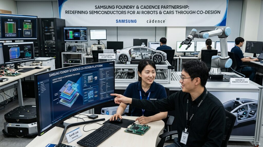
Automotive semiconductors face a harsher qualification environment than most consumer chips. They must withstand temperature extremes, long lifetimes, and stringent reliability standards. Viability depends not only on speed, but also on consistency over time. That is why suppliers with strong process control and validation culture hold an advantage in this sector.
There is a nuance here. The most advanced node is not always the best fit for every automotive or robotics design. Some controllers, safety units, and mixed-signal components remain better suited to mature nodes because of cost, reliability, or analog performance. The winning platform is the one that matches the application, not the one that looks best on a slide deck.
How Packaging Changes Product Architecture
Advanced packaging lets engineers place memory, compute, and interface blocks closer together, which reduces data movement and can improve performance per watt. In practical terms, that can mean better sensor processing for a robot or faster path planning in a driver-assistance platform. It also helps product teams manage scale, since different chiplet combinations can target different vehicle classes or robot tiers.
That flexibility is part of why semiconductor roadmaps are shifting. The old model favored one large SoC for as many functions as possible. The new model often favors modularity, because modularity gives teams better economics, faster iteration, and more ways to hit a performance target without redesigning the entire chip from scratch.
What Cadence Brings: EDA, Verification, and Multi-Die System Thinking
EDA is Where Risk Gets Reduced Before Silicon
Electronic design automation is the software layer that lets engineers simulate, place, route, analyze, and verify a chip before fabrication. In advanced AI programs, EDA is not a support tool; it is the control room. If the design flow fails to catch timing issues, power problems, or interconnect weaknesses early, the cost shows up later in lost wafers and missed launch windows.
Cadence is especially relevant because modern chips are no longer single-die problems. Multi-die systems require package-aware analysis, interconnect modeling, and verification across heterogeneous blocks. That makes the toolchain as important as the silicon itself.
Verification is the Difference Between Ambition and Shipment
Verification determines whether the chip actually behaves as intended. For automotive and robotics workloads, this includes more than functional correctness. It includes safety behavior, failover responses, timing under stress, and interactions between hardware and software. A design that passes one benchmark but fails a corner case is not ready for the field.
Cadence’s design and verification ecosystem is built around that reality. It helps teams close the gap between what the architecture promises and what the silicon can reliably deliver. That is especially useful when the product must operate in unpredictable environments, from dust-filled warehouses to busy urban traffic.
System-level Thinking Beats Isolated Optimization
The strongest part of Cadence’s position is that it encourages engineers to think at the system level. A chip is not successful because one block performs well in isolation. It succeeds when compute, memory, package, firmware, and power management all line up. This is where many programs fail: they optimize a single block and discover too late that the overall platform cannot sustain the workload.
Who works on large silicon programs knows this pattern well. The costliest mistakes are usually not dramatic design errors. They are coordination errors between teams, tools, and assumptions. A platform-level design flow reduces those errors before they become tape-out failures.
What This Means for the Semiconductor Market in 2025 And Beyond
AI Infrastructure is Moving Closer to the Edge
The semiconductor market is splitting into two broad directions: massive compute for data centers and specialized compute for the edge. Robots and AI vehicles belong to the edge category, but they are far more demanding than a typical IoT device. They need richer sensing, more robust inference, and stronger safety guarantees. That makes them a premium market for custom silicon and modular architectures.
Industry coverage of the Samsung-Cadence move, including reporting from TudoCelular’s report on chiplets and physical AI, reflects a broader trend: semiconductor value is shifting from raw transistor count to integrated system capability. The winners will be the companies that can align design tools, manufacturing, and packaging faster than competitors.
AI Cars and Robots Share the Same Silicon Logic
At first glance, automotive and robotics may look like separate markets. In reality, they share much of the same silicon logic: sensor fusion, real-time control, power efficiency, and safety-critical execution. That overlap is why a partnership like this has platform value. A successful architecture in one domain often transfers to the other with modifications, not a full redesign.
Samsung and Cadence Partnership Redefines Semiconductors for AI Robots and Cars because it treats the chip as part of a broader intelligent system, not as an isolated component. That view is becoming standard among leading hardware teams, especially those building products that must operate in the physical world rather than merely process data in the background.
External Signals Confirm the Strategic Direction
Samsung Newsroom regularly frames semiconductor progress around advanced nodes, AI, and next-generation applications, while Cadence’s newsroom highlights multi-die design, AI-assisted workflows, and domain-specific optimization. Academic work from institutions such as MIT also reinforces the central point: future compute is increasingly heterogeneous, tightly integrated, and application-specific.
One caution is worth stating plainly. Co-design partnerships improve the odds of success, but they do not eliminate manufacturing risk, software integration issues, or market mismatch. A platform can be technically elegant and still fail if the cost structure is wrong or the ecosystem is weak. That is why these alliances matter most when they are tied to real product pipelines, not just to roadmap slides.
Next Steps for Chip Strategy and Product Planning
Companies building robots, vehicles, or industrial AI systems should treat the Samsung-Cadence model as a blueprint for execution, not as a press-release curiosity. The real lesson is that silicon strategy now begins with the workload, then moves backward through architecture, packaging, verification, and manufacturing. If a team starts with node choice alone, it is already behind.
The most practical next step is to map workloads by latency, power, memory traffic, and safety requirement. That analysis reveals whether a design needs monolithic integration, chiplets, or a hybrid approach. From there, the team can decide how much of the stack needs custom silicon versus configurable IP, and where a foundry-EDA co-optimization flow can shorten the path to qualification.
For decision-makers, the direction is clear: prioritize system-level design partners, not just component vendors. The semiconductor advantage in physical AI will belong to organizations that can align architecture and manufacturing early, validate aggressively, and avoid over-optimizing for benchmark numbers that do not survive real-world deployment.
FAQ
What Does the Samsung-Cadence Partnership Change in Practical Terms?
It shortens and stabilizes the path from chip concept to manufacturable product. Samsung contributes process and packaging capability, while Cadence provides the tools to design, simulate, and verify complex silicon before fabrication. For AI robots and cars, that means fewer late-stage surprises, better power efficiency, and more realistic timing validation. The biggest gain is not a single feature; it is reduced integration risk across the entire development flow.
Why Are Chiplets Important for AI Robots and Autonomous Vehicles?
Chiplets let engineers divide a complex system into smaller, specialized dies connected through high-bandwidth interfaces. That improves modularity, yield, and product flexibility, which are all valuable when workloads vary across vehicle classes or robot platforms. It also helps manage memory and thermal constraints, which tend to become the limiting factors before raw compute runs out. In short, chiplets make the architecture easier to scale without forcing a full redesign.
Is Advanced-node Silicon Always the Best Choice for Automotive AI?
No. The newest node is not automatically the best fit for every automotive workload. Safety controllers, mixed-signal functions, and some power-sensitive components can still perform better on mature nodes because of cost, reliability, and analog behavior. The correct choice depends on the function, qualification target, and thermal budget. A strong semiconductor strategy uses the right node for the right block instead of chasing the smallest geometry everywhere.
Where Does Cadence Add the Most Value in This Type of Program?
Cadence adds the most value in early-stage modeling, verification, physical implementation, and multi-die analysis. Those are the stages where most design risk is exposed before tape-out. For AI and automotive chips, the ability to model timing, power, and package interactions early can save months of iteration and reduce wafer-level failures. That is especially important when the final product must meet strict safety and reliability requirements.
What is the Main Limitation of This Kind of Collaboration?
The main limitation is that co-optimization cannot fix a weak product strategy. If the workload is poorly defined, the software stack is immature, or the economics do not fit the target market, even excellent silicon tooling will not guarantee success. There is also a real tradeoff between performance, cost, and qualification complexity. The model works best when the company has a clear target application and a disciplined validation process.
How Does This Affect the Broader Semiconductor Market?
It reinforces a shift toward heterogeneous, application-specific compute. The market is moving away from generic chips as the default answer for everything and toward platforms built for specific physical AI workloads. That favors foundry and EDA ecosystems that can collaborate tightly across architecture, packaging, and verification. Over time, this should accelerate product cycles for robotics and vehicle intelligence while raising the bar for competitors.
Editorial Notice
This content was structured with the assistance of Artificial Intelligence and subjected to rigorous curation, fact-checking, and final review by Editor-in-Chief Nivailton Santos. TechTool Judge reaffirms its unyielding commitment to journalistic ethics, ensuring that editorial judgment and data validation remain entirely under human responsibility and final editorial oversight.